Product Detail
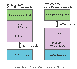
The complete Serial ATA controller has a fully optimized layer structure. It supports both host and device mode and is designed for a variety of applications. Figure 2 shows how customers can replace the application module with others, such as an Ethernet module or a PCI bridge.
The FTSATA320 and FXSATA303 solution has been tested extensively on the mature compliant test platform which is also available for customer to guarantee their own design compliance.
The IDE application layer translates IDE commands to Serial ATA and vice versa. Both ATA and ATAPI devices are supported. The transmission PIO mode is supported from 0 to 4. The IDE application layer adopts the State machine based design without embedded CPU core making it very competitive in the final die size. Furthermore, the IDE application layer has been proven to be 100% compatible with Windows and Linux operating systems without any driver support.
The transport layer has a built-in configurable FIFO. The Rx FIFO can be configured to select from 8/16/32 double words. Its function is to assemble and decompose SATA data packet to and from the link layer. The ATA/ATAPI related shadow registers are responsible to continuously maintain the data compatibility. The link layer is designed to support 10/20/40-bit data interfaces.
FXSATA303, the Serial ATA PHY Layer
Faraday's SATA PHY supports dual operating speeds (1.5G and 3.0G) with speed negotiation function. The low jitter PLL design guarantees very low bus error rate. The integrated BIST and the loop back function eliminate the need for high speed test equipment. It provides a low speed interface to the link layer by a 20/40-bit data bus. FXSATA303 0.18µm process version PHY is available now.
The 0.13µm HS process version PHY is designed to fit into the IO-pad ring, saving valuable core space while reducing costs. The size of an one port PHY is only 0.45 mm2. With the ultra low power design, and the smallest die size, Faraday's SATA solution can help users deliver the most competitive products.
Highlights
- 3Gb/s SATA transceiver in 0.18m/0.13m UMC process
- Compliant with SATA-II specification
- Link and transport layer together are 30K gates
- Supports 10/20/40-bit PHY interface
- Supports K28.5 comma detection
- OOB signal detection and transmission
- Signal clock to link layer: 75MHz at 3.0G and 37.5MHz at 1.5G
- Slumber, partial power mode support
- Fully partitioned layered structure
- Configurable FIFO width in transport layer
- Application layer complies with ATA/ ATAPI standards
|


